|
|
| ATM Ring Switch - Synchronization System
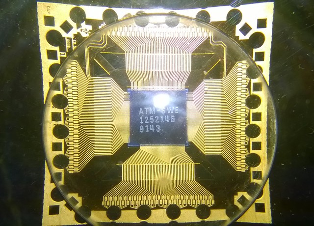
This was one of my major project. In 1993 I was involved in a new development activity based on a new generation of digital switch for public communication networks, the ATM Ring Switch. This project was named "P3A" and it was designed basically around a new high-speed digital chip made by Ellemtel-Ericsson, the Switch Element (SWE, see the above picture).
I was the HW designer of the synchronization system (SSY) of the switch nodes and the high speed electrical node interfaces (COBs, the Communication Boards).
The Synchronization System was made by using two Clock Boards (CBs, for redundancy reasons), configured as master and slave depending from the position where they were inserted into the mainframe, and one CSCB (Clock Selection and Connection Board).
The CB schematic can be viewed by clicking HERE, the CSCB schematic is available HERE and finally HERE is available the schematic of the COB unit.
And HERE there are the slides I prepared to show the overall ATM Ring Switch system by using some block diagrams.
You are here: Home-My projects-SSY ATM Switch Previous Topic: Stereo dig. limiter Next Topic: S.Marco DECT RFP
|


